
In the fast-paced world of electronics, precision and speed are paramount when designing a new product. The prototyping stage, particularly the PCB prototype phase, is one of the most crucial steps in turning your innovative ideas into tangible devices. Whether you're working on a consumer gadget, a medical device, or an industrial machine, mastering the PCB design process can make or break the success of your project.
In this article, we’ll dive into the importance of PCB prototypes, explore the steps involved in the design process, and offer some tips on how to ensure a high-quality, reliable design. If you're looking to enhance your prototyping skills, find out more below!
Understanding the Importance of PCB Prototypes
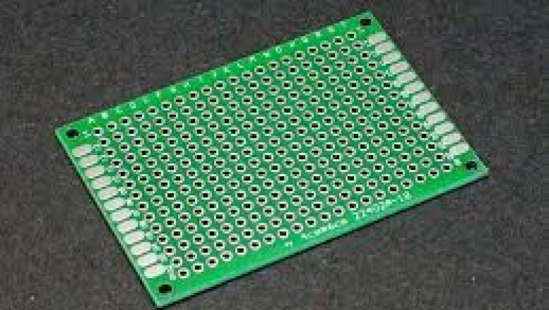
Before we get into the nitty-gritty of PCB design, it’s important to understand what a PCB prototype is and why it’s such a critical part of the development process. A PCB (Printed Circuit Board) is the backbone of most electronic devices, serving as the platform where components such as resistors, capacitors, chips, and connectors are placed to form a complete circuit.
A PCB prototype is essentially a preliminary version of the final circuit board that is built to test the functionality, fit, and performance of the design. It allows engineers to check for issues like incorrect routing, component placement errors, or electrical connectivity problems before committing to full-scale production. Without a prototype, you're essentially gambling with the final product, risking costly delays and design flaws.
In essence, a PCB prototype ensures that the final product works as intended and that any potential issues are caught early in the design phase.
The Key Steps in the PCB Design Process
Designing a high-quality PCB prototype requires a combination of technical knowledge, attention to detail, and a structured approach. Let’s break down the process into its key steps.
1. Conceptualization and Specifications
The first step in the PCB design process is defining the project's requirements. This includes understanding the electronic functionality, power requirements, and physical constraints of the device. At this stage, the designer should answer questions like:
- What components are required?
- What are the size and shape constraints?
- What is the operating voltage and current?
- What environment will the PCB be used in (e.g., high temperature, high vibration)?
This is the stage where engineers create a specification sheet for the board, which will guide all future decisions in the design process. If you’re new to PCB design, it’s a good idea to check over here for detailed guides on creating PCB specifications.
2. Schematic Design
Once the specifications are clear, the next step is to create the schematic diagram, which acts as the blueprint for the entire PCB design. The schematic will show how the components are connected to each other and ensure that the circuit functions as intended.
During this phase, it’s crucial to pick components that are compatible with each other. Using an electronic design automation (EDA) tool can help visualize and simulate the circuit. These tools can detect errors early in the design process and provide feedback on electrical performance.
3. PCB Layout Design
After finalizing the schematic, the next step is to convert it into a physical layout. This is where the design takes shape as a PCB prototype. The designer places the components on the board and routes the electrical connections between them. It’s a delicate balance between efficiency and precision. Proper routing ensures the signals can travel with minimal interference and loss.
In this step, several factors need to be considered, such as:
- Trace Width and Spacing: Traces should be thick enough to handle the current but not so wide as to take up excessive space. Similarly, spacing between traces is essential to avoid short circuits.
- Layer Stack-up: For more complex designs, you may need to design multi-layer PCBs. The right stack-up can ensure optimal signal integrity and heat dissipation.
- Thermal Management: High-power components may generate heat that can damage the board if not managed properly. Thermal vias and heat sinks are common solutions for this issue.
At this stage, it’s essential to use the correct tools and techniques to avoid mistakes. Many professionals go right here to industry-standard software to handle complex layouts.
4. Design Rule Check (DRC)
After completing the layout, the next step is performing a Design Rule Check (DRC). This process ensures that the design meets the manufacturing standards for trace width, spacing, and component placement. It also checks for electrical errors such as unconnected nets or incorrect vias.
DRC is an essential step in avoiding errors that could affect the manufacturability or performance of the final product. Automated tools can help catch many of these issues, but it’s also a good idea to manually review the design before moving forward.
5. Prototype Manufacturing and Testing
Once the design passes the DRC, it’s time to send the files to a manufacturer to create the PCB prototype. Typically, manufacturers use the Gerber files generated by the design software to produce the actual PCB. This stage usually involves a small batch of prototypes, which are tested for functionality.
Testing is crucial, as it allows engineers to identify any problems that weren’t apparent during the design process. It’s an iterative phase where adjustments may need to be made before proceeding to full-scale production.
6. Final Revisions and Production
After testing the prototype and identifying any issues, engineers make the necessary revisions to the design. Once the design is refined and verified, it’s ready for full production. This can involve sourcing the final components and assembling the boards into the finished product.
Best Practices for a Successful PCB Prototype
Designing a successful PCB prototype isn’t just about following the steps above—there are best practices that can make your design process smoother and more efficient. Here are some tips:
Plan for Testing Early
Design with testing in mind. Consider including test points for key signals, and make sure there’s space for probes or test fixtures. This will make the testing process easier and faster once the prototype is built.
Keep Track of Component Availability
There’s nothing worse than designing a board, only to realize that the components you chose are no longer available or have long lead times. Always check component availability before finalizing the design.
Use a Modular Approach
When possible, design the PCB in a modular way. This allows you to reuse parts of the design in future projects, saving time and effort. It also reduces the likelihood of design errors that might arise when creating a completely custom solution from scratch.
Minimize Complexity
While it’s tempting to add fancy features to your design, simplicity often leads to a more reliable and cost-effective product. Avoid unnecessary complexity, and focus on achieving the core functionality of your device.
Conclusion
Mastering the PCB design process is essential for creating successful electronic products. From the initial conceptualization to the final prototype testing, every step plays a vital role in ensuring that your device functions as expected. A well-designed PCB prototype not only identifies potential problems early but also sets the stage for the production of high-quality, reliable electronic devices.
Whether you’re a seasoned professional or just starting out, these insights into the PCB design process can help you improve your prototyping skills. And if you want to dive deeper into each step, find out more about specific tools, techniques, and tips to ensure success.


Comments
0 comment